Description of printed circuit boards
A printed circuit board implies a structure of electrical interconnections that are made on an insulating base (dielectric – fiberglass, getinax, ceramic base, etc.). The printed circuit board, together with the electronic components (products) installed and mounted on it, forms a printed circuit assembly. The conductors of a printed circuit board lying in the same plane are called a printed pattern, a layer. According to the functions they perform, the PP layers are divided into: signal (information), potential (grounding, power), shielding and technological layers of conductors; according to the structural arrangement on the board – internal and external layers by CAMTECH PCB. In addition to conductors (called tracks), the boards contain:
Installation mounting elements: pads and mounting holes;
Fixing (basic) elements for aligning the terminals of electronic component cases with contact pads or mounting holes on a printed circuit board;
Printed lamellas for contact with connectors;
Heat-removing and heat-leveling sections;
Marked layers;
Technological contact pads;
Solder masks – heat-resistant electrically insulating film coating;
Circuit elements performed by printing methods: inductance, capacitance, resistance.
Depending on the purpose and production capabilities, printed circuit boards are made single-sided, double-sided or multilayer, on a rigid or flexible base.
Single-sided printed circuit boards
Single-sided printed circuit boards are an insulating base, on one side of which a conductive pattern is made. Through non-metallized holes are used for mechanical fixation of pin components in the board, and for connection – contact pads, which end all printed conductors. Tracing conductors on the same surface (in the same layer, in the same level) does not allow you to resolve the conflict of intersecting traces otherwise than by setting wire jumpers.
Double-sided printed circuit boards
A double-sided printed circuit board has one base, on both sides of which conductive patterns are made, and all the required electrical connections of the two sides are connected mainly through metallized holes. The conflict of crossing connections is solved here by the possibility of transferring the conflicting trace around to the other side of the printed circuit board using plated holes. Such a hole for transferring the route is called a transition hole, in contrast to the mounting hole. In this case, the design of the via can be arbitrary, and the mounting hole can be according to the norms for the formation of a solder assembly.
However, trace conflicts are not completely resolved: the power and ground circuits, the mounting field for connecting the outputs of multi-output components (microcircuits) interfere with the free placement of signal traces. This contention is partially resolved in four interconnection layers.
Multilayer printed circuit boards
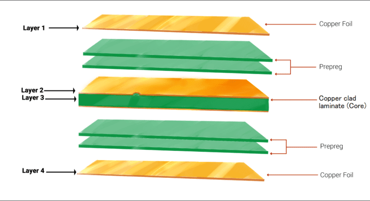
Four-layer printed circuit boards contain potential circuits (power and ground) on the inner layers, and signal traces and a mounting field for connecting components on the outer (outer) layers. It is advantageous to design four-layer printed circuit boards in such a way that they can be manufactured using double-sided technology.
So multilayer pcb contain alternating layers of thin insulating substrates with conductive patterns deposited on them, physically connected into one multilayer base. Electrical connections in the MPP multilayer structure are made through (mainly) or blind holes. Each of the internal layers can be a single-sided board or a double-sided board with vias.
Description of the layers of multilayer printed circuit boards
Layers in MPP have a specific functional purpose:
Outer mounting layers are designed and used for mounting electronic components;
Signal layers, carry the topological scheme of signal interconnections;
The ground and power layers are usually made as large polygons with minimal ohmic and inductive resistances, they simultaneously serve as electrical screens grounded at high frequency by decoupling capacitances;
Heat-removing or heat-leveling layers.
The increase in packing density associated with this increase in the number of interconnects was usually solved by increasing the layers. There are examples of creating 40 or more layer printed circuit boards.
Priorities for Increasing the Number of Multilayer PCB Interconnects
Today, the predominant direction of increasing the number of interconnections:
Increase in the density of traces by reducing the routing step with a simultaneous decrease in the width of the conductors;
Performing interlayer transitions in the trace step, that is, in the dimensions of thin conductors;
Performance of multilevel interconnections in multilayer structures: through, blind, deaf.
Flexible printed circuit boards
Flexible printed circuit boards, in the implementation of interconnections, are similar to single-sided, double-sided and multilayer, with the difference that the insulating and metal layers are made thin, for flexibility, from materials that can withstand repeated bending.


